Understanding Surface Roughness
Authors: Victoria Marcune,Shawn Iles
Surface roughness is one component of describing how the shape of a surface deviates from its ideal form, where higher values correspond to rougher surfaces while lower values indicate the surface is smooth. Roughness describes high spatial frequency errors, meaning very small deviations on the order of Angstroms (10-10 m). Understanding the surface roughness of optical surfaces is critical to control light scatter, as scatter can be proportional to the surface roughness of the optics. Light scattering and absorption from surface roughness have a significant impact on applications such as high-power laser systems, which can negatively impact the efficiency and laser damage threshold. In addition to impacting damage threshold, scattered high-power laser radiation can be a safety hazard for anyone near the system, as the light is being redirected in unintended directions. The current standard utilized for surface roughness is ISO 10110-8, which defines how surface roughness should be analyzed and specified.
Reading Surface Roughness Callouts
An ISO 10110-8 compliant drawing will list the following specifications to give a complete description of the optical surface.

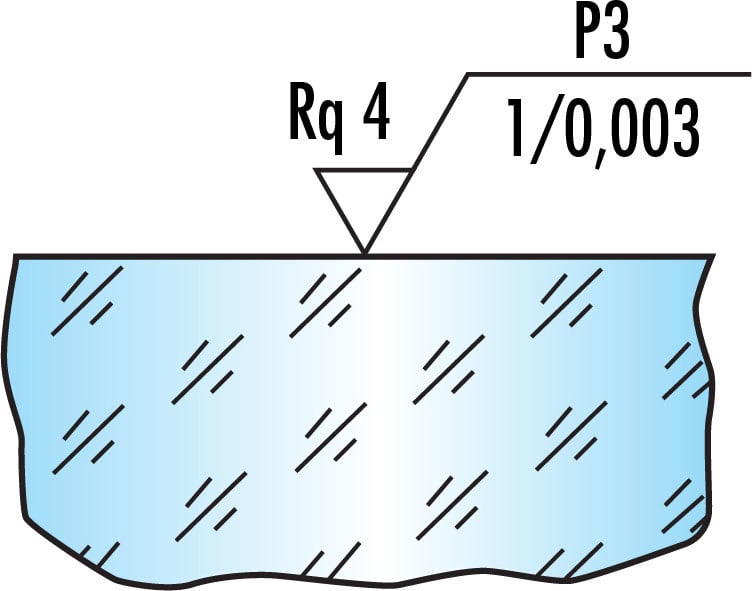
Figure 1: Example surface roughness specification
Surface Finish, shown in Figure 1 as "P3":
This variable indicates the surface finish. For simple polishing specifications, it could either be a G, for ground surface, or P to indicate it is optically polished. The grade of the polishing will be assigned from 1-4 according to the degree of smoothness in terms of microdefects per 10mm scan as shown below in Table 1:
| Polishing Grade Designation | Number, N, of Microdefects per 10mm of Sampling Length |
|---|---|
| P1 | 80 ≤ N < 400 |
| P2 | 16 ≤ N < 80 |
| P3 | 3 ≤ 16 |
| P4 | N < 3 |
Table 1: Indication of the degree of smoothness in terms of microdefects
Statistical method used, shown in Figure 1 as "Rq 4":
This will indicate the statistical method used to measure the surface roughness, followed by the value.
Spatial bandwidth, shown in Figure 1 as "1/0.003":
This specifies the spatial bandwidth ranging from the upper bound to the lower bound.
Spatial Frequencies and Frequency Groups
When quantifying the surface texture of an optical component, it is important to define what level of spatial resolution is being measured. Surface texture, or the complete shape of a surface, can be broken down into three main spatial frequency groups: roughness, waviness, and figure.

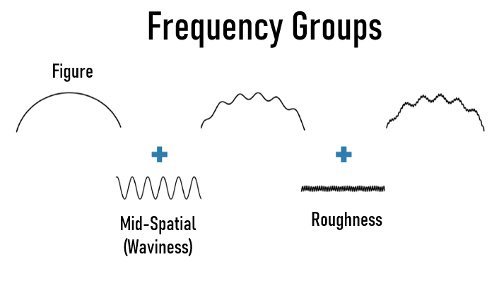
Figure 2: Figure, waviness, and roughness characterize surface texture at different scales
Figure 2 shows how surface figure, waviness, and roughness together characterize all of the ways a surface deviates from its ideal shape. Figure describes the overall shape of the surface and is the largest scale, or largest spatial frequencies, which will be analyzed. The errors described by figure are on the order of tenths of mm to cm. Waviness measures mid-spatial frequency errors describing features on the order of µms to mm. Roughness is the smallest form of error and describes closely-spaced abnormalities in the surface texture on the order of tenths of Angstroms to tens of µm.
ISO 10110-8 Surface Roughness Parameters
The goal of ISO 10110-8 is to specify rules for how the surface texture is to be defined. According to ISO, “Surface texture is the characteristic of a surface that can be effectively described with statistical methods”. The ISO standard outlines 5 statistical methods which are used to describe optically-smooth surfaces. These methods can be used in combination and also over various spatial bandwidths. Defining the upper and lower bounds of the spatial frequency is critical to obtaining accurate results. If no spatial frequency is defined, ISO 10110-8 standards specify an assumed range of 0.0025mm – 0.08mm.
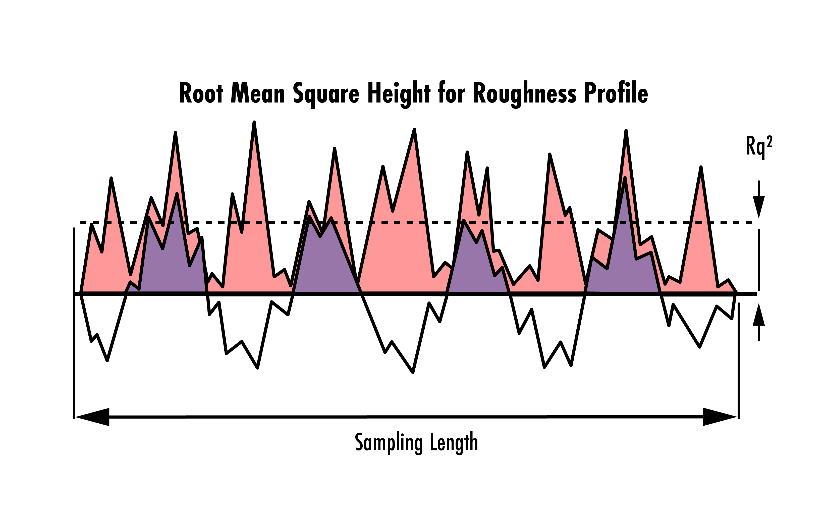
1 & 2. RMS roughness and waviness: The root mean square (RMS) method is the most common way optically-smooth surfaces are specified in the United States, while in Europe it is more common to specify absolute roughness. The RMS average of profile height deviations from the mean line is utilized to statistically analyze the smoothness of an optical surface. RMS roughness, $ Rq $, refers to the roughness profile while RMS waviness, $ Wq $, refers to the waviness profile. Both are measured using the same RMS method, but over different spatial frequencies.

Figure 3: Example of a roughness profile measured over a given sampling length. The Rq2 indicates the root mean square height
3. RMS Slope: Similar to the RMS roughness and waviness, optically-smooth surfaces can be specified using the RMS slope of the local tilt, $ \tfrac{\text{d} Z \left( x \right)}{\text{d}x} $, of the surface along a given sampling length.
$$ \begin{pmatrix} T\\ T \Delta q \end{pmatrix} = \begin{Bmatrix} \begin{pmatrix} Rq\\ R \Delta q \end{pmatrix} \text { for } 1 \large{\unicode[computer modern]{x212B}} \leq lr\leq 1 \large{\unicode[computer modern]{x03BC}} \normalsize{\text{m}} \\ \begin{pmatrix} Wq\\ W \Delta q \end{pmatrix} \text { for } 1 \large{\unicode[computer modern]{x03BC}} \normalsize{\text{m}} < lr\leq 1 \text{mm} \end{Bmatrix} $$
$$ \begin{pmatrix} T\\ T \Delta q \end{pmatrix} = \begin{Bmatrix} \begin{pmatrix} Rq\\ R \Delta q \end{pmatrix} \text { for } 1 \large{\unicode[computer modern]{x212B}} \leq lr\leq 1 \large{\unicode[computer modern]{x03BC}} \normalsize{\text{m}} \\ \begin{pmatrix} Wq\\ W \Delta q \end{pmatrix} \text { for } 1 \large{\unicode[computer modern]{x03BC}} \normalsize{\text{m}} < lr\leq 1 \text{mm} \end{Bmatrix} $$
(Scroll right to see full equation)
4. Indication of density of microdefects: Microdefects are the pits and scratches which can be found on an optically-smooth surface. They are commonly quantified using an optical profilometer, a microscope, or a microscopic image comparator. ISO 10110-8 states that “the number of microdefects, $ N $, is taken to be over a 10mm line scan with a resolution of 3 µm, or an area of 300µm $ \times $ 300µm with the same resolution.”
5. Power spectral density (PSD) function: The PSD function is one of the most comprehensive statistical methods for measuring surface roughness. It allows for a complete description of the surface texture characteristics by providing the relative strength of each roughness component as a function of spatial frequency.
(Scroll right to see full equation)
This is the general equation used to calculate the PSD of a 2-dimensional surface. $ f_x $ and $ f_y $ are the spatial frequencies of the surface texture $ z \! \left( x, y \right) $, which is defined over a square area of side length, $ L $.
Metrology For Measuring Surface Roughness
There is a range of metrology technologies that are uniquely suited for different spatial frequencies. The most common are conventional interferometry, white light interferometry, and atomic force microscopy. Figure 4 below demonstrates which regions and wavelengths are best suited for these technologies.

Figure 4: Spatial frequency range of typical metrology equipment.
Conventional interferometry is ideal for measuring low spatial frequency errors. This class of surface errors is referred to as figure errors and is associated with typical Zernike polynomials. Zernike polynomials describe errors caused by wavefront aberrations as an optical component deviates from an ideal shape. A white light interferometer is best suited to measure waviness or mid-range spatial frequency errors. Waviness is often attributed to creating effects such as hazing and decreased contrast. Finally, the atomic force microscope provides the best resolution for high-frequency spatial errors which characterize the roughness of the optical surface. There are some overlaps in these groups, as both the white light interferometer and the atomic force microscope can be used to measure roughness. The correct choice of equipment will be partially dependent on the wavelength of the application. For example, WLI is ideal when measuring visible or IR spectra as they are typically analyzed at frequencies less than 2,000 cycles/mm.
Specifying Surface Quality for Ultrafast Optics
When analyzing ultrafast optics, manufacturers must use their discretion to specify surface quality as there is currently no standard for doing so. Several ultrafast optics manufacturers specify only pre-coating surface quality while other manufacturers may only quote 20-10 or above post-coating.
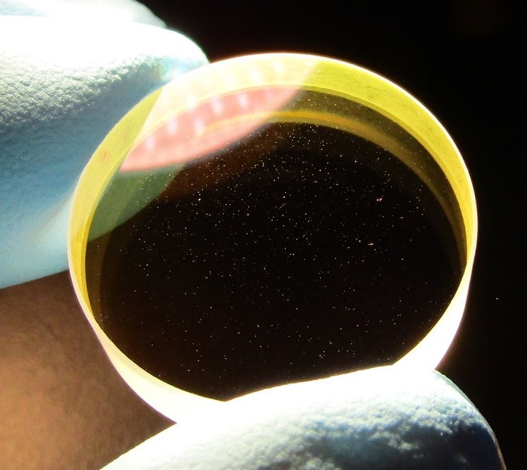
Optics created for ultrafast applications typically feature thick, specialized coatings that require a long sputtering process. Due to the length of this process, imperfections can be sputtered within the coating which leads to a cosmetic appearance of "dust" or otherwise irregular surface quality. Rather than dust, these imperfections are created by small surges in the flow of the material being sputtered. Throughout the duration of the coating process, there can be variations in sputtering rate which result in local microdeposits of the coating

Figure 5: Typical appearance of an optic with an ultrafast coating. Despite the appearance of irregular surface quality, Edmund Optics guarantees the specified performance of our ultrafast optics.
Despite their appearance, these imperfections have negligible effects on the overall performance of the optic. Due to the relatively small size of these imperfections, the affected portions of the beam become insignificant when considering the bulk properties of the film such as group delay dispersion and reflectivity. While negligible in most circumstances, applications that require small beam sizes or ultralow loss may suffer from an increase in scattering through the system from these imperfections. To meet tighter specifications, special measures can be taken to reduce overall scatter such as starting with a super-polished substrate.
Metrology at Edmund Optics®
Measuring what you make is a key component of manufacturing. Edmund Optics utilizes a strict global quality program to ensure components meet their specified requirements. A range of equipment including interferometers, profilometers, coordinate measurement machines (CMM), and a host of other optical and mechanical metrology devices are utilized to perform in-house testing to determine surface roughness and other optical properties. To learn more about our custom metrology capabilities, please visit our metrology capabilities webpage.
References
- ISO 10110-8:2019, Optics and photonics — Preparation of drawings for optical elements and systems — Part 8: Surface texture
- Filhaber, John. “LARGE OPTICS: Mid-Spatial-Frequency Errors: The Hidden Culprit of Poor Optical Performance.” Laser Focus World, 13 Aug. 2013
- “Root Mean Square Slope (Rδq, Pδq, Wδq): Surface Roughness Parameters.” Root Mean Square Slope (Rδq, Pδq, Wδq) | Surface Roughness Parameters | Introduction To Roughness | KEYENCE America
- Deck, Leslie L., and Chris Evans. “High Performance Fizeau and Scanning White-Light Interferometers for Mid-Spatial Frequency Optical Testing of Free-Form Optics.” Advances in Metrology for X-Ray and EUV Optics, 2005, https://doi.org/10.1117/12.616874.
- Jayson Nelson, Shawn Iles, "Creating sub angstrom surfaces on planar and spherical substrates," Proc. SPIE 11175, Optifab 2019, 1117505 (15 November 2019); https://doi.org/10.1117/12.2536689


or view regional numbers
QUOTE TOOL
enter stock numbers to begin
Copyright 2023 | Edmund Optics, Ltd Unit 1, Opus Avenue, Nether Poppleton, York, YO26 6BL, UK
California Consumer Privacy Acts (CCPA): Do Not Sell or Share My Personal Information
California Transparency in Supply Chains Act